- 您现在的位置:买卖IC网 > Sheet目录287 > 24LC21A/P (Microchip Technology)IC EEPROM 1KBIT 400KHZ 8DIP
�� �
�
�24LC21A�
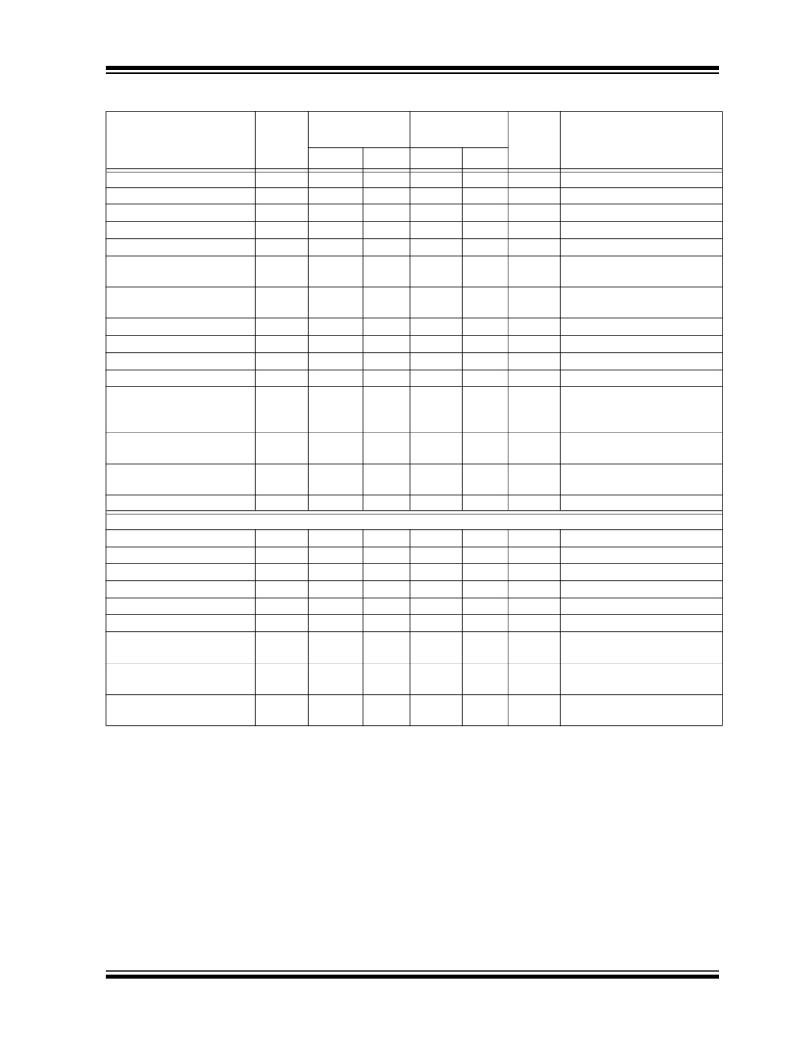
�TABLE� 1-2:�
�AC� CHARACTERISTICS�
�Vcc� =� 2.5-5.5V�
�Vcc� =� 4.5� -� 5.5V�
�Parameter�
�Symbol�
�Standard� Mode�
�Min.�
�Max.�
�Fast� Mode�
�Min.�
�Max.�
�Units�
�Remarks�
�Clock� frequency�
�Clock� high� time�
�Clock� low� time�
�F� CLK�
�T� HIGH�
�T� LOW�
�—�
�4000�
�4700�
�100�
�—�
�—�
�—�
�600�
�1300�
�400�
�—�
�—�
�kHz�
�ns�
�ns�
�SDA� and� SCL� rise� time�
�SDA� and� SCL� fall� time�
�Start� condition� hold� time�
�T� R�
�T� F�
�T� HD� :� STA�
�—�
�—�
�4000�
�1000�
�300�
�—�
�—�
�—�
�600�
�300�
�300�
�—�
�ns�
�ns�
�ns�
�(Note� 1)�
�(Note� 1)�
�After� this� period� the� first� clock�
�pulse� is� generated�
�Start� condition� setup� time�
�T� SU� :� STA�
�4700�
�—�
�600�
�—�
�ns�
�Only� relevant� for� repeated�
�Start� condition�
�Data� input� hold� time�
�Data� input� setup� time�
�Stop� condition� setup� time�
�Output� valid� from� clock�
�Bus� free� time�
�T� HD� :� DAT�
�T� SU� :� DAT�
�T� SU� :� STO�
�T� AA�
�T� BUF�
�0�
�250�
�4000�
�—�
�4700�
�—�
�—�
�—�
�3500�
�—�
�0�
�100�
�600�
�—�
�1300�
�—�
�—�
�—�
�900�
�—�
�ns�
�ns�
�ns�
�ns�
�ns�
�(Note� 2)�
�(Note� 2)�
�Time� the� bus� must� be� free�
�before� a� new� transmission�
�can� start�
�Output� fall� time� from� V� IH�
�T� OF�
�—�
�250�
�20� +� 0.1�
�250�
�ns�
�(Note� 1)� ,� C� B� ≤� 100� pF�
�minimum� to� V� IL� maximum�
�C� B�
�Input� filter� spike� suppres-�
�T� SP�
�—�
�50�
�—�
�50�
�ns�
�(Note� 3)�
�sion� (SDA� and� SCL� pins)�
�Write� cycle� time� T� WR�
�—�
�10�
�—�
�10�
�ms�
�Byte� or� Page� mode�
�Transmit-Only� Mode� Parameters�
�Output� valid� from� VCLK� T� VAA�
�VCLK� high� time� T� VHIGH�
�VCLK� low� time� T� VLOW�
�VCLK� setup� time� T� VHST�
�VCLK� hold� time� T� SPVL�
�Mode� transition� time� T� VHZ�
�—�
�4000�
�4700�
�0�
�4000�
�—�
�2000�
�—�
�—�
�—�
�—�
�1000�
�—�
�600�
�1300�
�0�
�600�
�—�
�1000�
�—�
�—�
�—�
�—�
�500�
�ns�
�ns�
�ns�
�ns�
�ns�
�ns�
�Transmit-only� power-up�
�T� VPU�
�0�
�—�
�0�
�—�
�ns�
�time�
�Input� filter� spike� suppres-�
�T� SPV�
�—�
�100�
�—�
�100�
�ns�
�sion� (VCLK� pin)�
�Endurance� —�
�1M�
�—�
�1M�
�—�
�cycles�
�25°C,� Vcc� =� 5.0V,� Block�
�mode� (Note� 4)�
�Note� 1:�
�2:�
�3:�
�4:�
�Not� 100%� tested.� C� B� =� Total� capacitance� of� one� bus� line� in� pF.�
�As� a� transmitter,� the� device� must� provide� an� internal� minimum� delay� time� to� bridge� the� undefined� region�
�(minimum� 300� ns)� of� the� falling� edge� of� SCL� to� avoid� unintended� generation� of� Start� or� Stop� conditions.�
�The� combined� T� SP� and� V� HYS� specifications� are� due� to� Schmitt� Trigger� inputs� which� provide� noise� and�
�spike� suppression.� This� eliminates� the� need� for� a� T� I� specification� for� standard� operation.�
�This� parameter� is� not� tested� but� ensured� by� characterization.� For� endurance� estimates� in� a� specific�
�application,� please� consult� the� Total� Endurance?� Model� which� can� be� obtained� from� Microchip’s� web� site�
�at� www.microchip.com.�
�?� 2008� Microchip� Technology� Inc.�
�DS21160G-page� 3�
�发布紧急采购,3分钟左右您将得到回复。
相关PDF资料
24LC22A-I/P
IC EEPROM 2KBIT 400KHZ 8DIP
24LC64XT-I/ST
IC SERIAL EEPROM 64K 2.5V 8TSSOP
24LCS21A/P
IC EEPROM 1KBIT 400KHZ 8DIP
24LCS22A-I/P
IC EEPROM 2KBIT 400KHZ 8DIP
24VL014/SN
IC EEPROM 1KBIT 400KHZ 8SOIC
24VL014H/SN
IC EEPROM 1KBIT 400KHZ 8SOIC
24VL024/SN
IC EEPROM 2KBIT 400KHZ 8SOIC
24VL024H/SN
IC EEPROM 2KBIT 400KHZ 8SOIC
相关代理商/技术参数
24LC21A/SN
功能描述:电可擦除可编程只读存储器 2.5V Dual Mode RoHS:否 制造商:Atmel 存储容量:2 Kbit 组织:256 B x 8 数据保留:100 yr 最大时钟频率:1000 KHz 最大工作电流:6 uA 工作电源电压:1.7 V to 5.5 V 最大工作温度:+ 85 C 安装风格:SMD/SMT 封装 / 箱体:SOIC-8
24LC21A/SN
制造商:Microchip Technology Inc 功能描述:IC SM EEPROM SERIAL 1K
24LC21A-I/P
功能描述:电可擦除可编程只读存储器 2.5V Dual Mode RoHS:否 制造商:Atmel 存储容量:2 Kbit 组织:256 B x 8 数据保留:100 yr 最大时钟频率:1000 KHz 最大工作电流:6 uA 工作电源电压:1.7 V to 5.5 V 最大工作温度:+ 85 C 安装风格:SMD/SMT 封装 / 箱体:SOIC-8
24LC21A-I/PG
功能描述:电可擦除可编程只读存储器 2.5V Dual Mode Lead Free Package
RoHS:否 制造商:Atmel 存储容量:2 Kbit 组织:256 B x 8 数据保留:100 yr 最大时钟频率:1000 KHz 最大工作电流:6 uA 工作电源电压:1.7 V to 5.5 V 最大工作温度:+ 85 C 安装风格:SMD/SMT 封装 / 箱体:SOIC-8
24LC21A-I/SN
功能描述:电可擦除可编程只读存储器 2.5V Dual Mode RoHS:否 制造商:Atmel 存储容量:2 Kbit 组织:256 B x 8 数据保留:100 yr 最大时钟频率:1000 KHz 最大工作电流:6 uA 工作电源电压:1.7 V to 5.5 V 最大工作温度:+ 85 C 安装风格:SMD/SMT 封装 / 箱体:SOIC-8
24LC21A-I/SNG
功能描述:电可擦除可编程只读存储器 2.5V Dual Mode Lead Free Package
RoHS:否 制造商:Atmel 存储容量:2 Kbit 组织:256 B x 8 数据保留:100 yr 最大时钟频率:1000 KHz 最大工作电流:6 uA 工作电源电压:1.7 V to 5.5 V 最大工作温度:+ 85 C 安装风格:SMD/SMT 封装 / 箱体:SOIC-8
24LC21AT/SN
功能描述:电可擦除可编程只读存储器 2.5V Dual Mode RoHS:否 制造商:Atmel 存储容量:2 Kbit 组织:256 B x 8 数据保留:100 yr 最大时钟频率:1000 KHz 最大工作电流:6 uA 工作电源电压:1.7 V to 5.5 V 最大工作温度:+ 85 C 安装风格:SMD/SMT 封装 / 箱体:SOIC-8
24LC21AT/SN-CUT TAPE
制造商:Microchip 功能描述:24LC21 Series 1 Kb I2C 2 Wire (128 x 8) 2.5V Serial EEPROM SMT - SOIC-8